Ion Beam Etching Pdf
.jpg)
An Introduction To Ion Beam Etching

Dry Etch Processes Dryetching Semiconductor Technology From A To Z Halbleiter Org
Ion Beam Lithography

Pdf Ion Beam Figuring Of Optics
Https Www Tf Uni Kiel De Matwis Afm Download Mst Ws2018 Dry Etching 2018 Pdf

Electronic Transport In Helium Ion Beam Etched Encapsulated Graphene Nanoribbons Sciencedirect
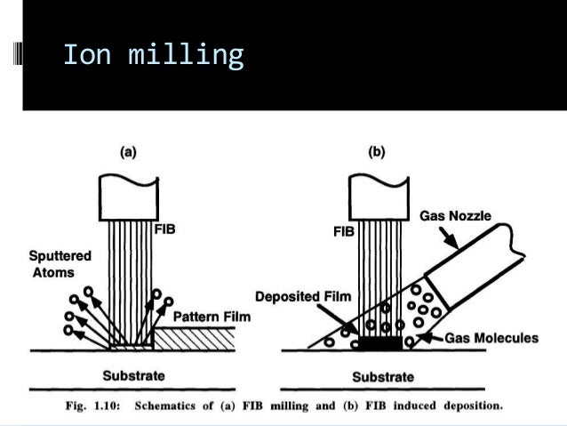
Ion beam etching or milling is achieved by directing a beam of charged particles ions at a substrate with a suitably patterned mask in a high vacuum chamber.
Ion beam etching pdf.

Focused Ion Beam An Overview Sciencedirect Topics
Https Iopscience Iop Org Article 10 1088 1742 6596 1407 1 012083 Pdf

Pdf Focused Ion Beam Lithography

Reactive Ion Beam Etching Of Large Diffraction Gratings Plymouth Grating Laboratory

Non Contact Polishing Of Single Crystal Diamond By Ion Beam Etching Sciencedirect

Ion Beam An Overview Sciencedirect Topics
Http Www Vacuum Uk Org Pdfs Vs7 Vacuumquality Dpearson Pdf

Fine Tuning The Etch Depth Profile Via Dynamic Shielding Of Ion Beam Sciencedirect

Focused Ion Beams And Some Selected Applications Machalett Major Reference Works Wiley Online Library

Pdf Overview Of Etching Technologies Used For Hgcdte

Pdf A Survey On The Reactive Ion Etching Of Silicon In Microtechnology
Https Iopscience Iop Org Article 10 1088 1361 6528 Aaf521 Pdf

Effect Of Ion Beam Etching On The Surface Roughness Of Bare And Silicon Covered Beryllium Films Sciencedirect

Reactive Ion Etching Cf4 Ar And Ion Beam Etching Of Various Glasses For Diffractive Optical Element Fabrication Schmitt 2018 International Journal Of Applied Glass Science Wiley Online Library
Pdf Etching Characteristics Of Linbo3 In Reactive Ion Etching And Inductively Coupled Plasma
Http Pubs Acs Org Doi Pdf 10 1021 Acsami 6b09758

Pdf Electron Beam Lithography And Plasma Etching To Fabricate Supports For Studying Nanomaterials
Pdf Overview Of Atomic Layer Etching
1

Pdf Reactive Ion Etching Of Quartz And Silica Based Glasses In Cf 4 Chf 3 Plasmas
Ion Beam Deposition Ibd Oxford Instruments

Implementation Of Smooth Nanocrystalline Diamond Microstructures By Combining Reactive Ion Etching And Ion Beam Etching Sciencedirect

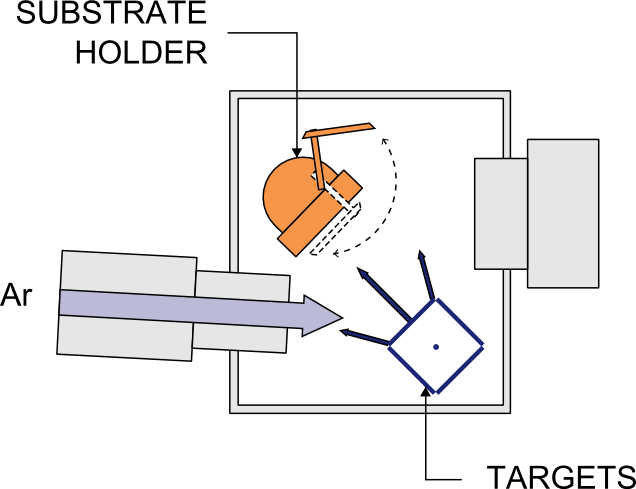
Ion Beam Machining Ion Implantation Sputtering

Pdf Investigation Of Reactive Ion Etching Of Dielectrics And Si In Chf3 O2 Or Chf3 Ar For Photovoltaic Applications Semantic Scholar

Ewdlpe7hdopngm

Iii Wet And Dry Etching Pdf Free Download

Focused Ion Beam Etching Of Gan
Pdf Dry Etching Of Carbon Layers In Various Etch Gases
Https Avs Scitation Org Doi Pdf 10 1116 1 4932161

Ion Beam Assisted Deposition An Overview Sciencedirect Topics

Pdf Application Of Focused Ion Beam Micromachining A Review

Plasma Etching In Microelectronics Sciencedirect

Pdf Tutorial The Systematics Of Ion Beam Sputtering For Deposition Of Thin Films With Tailored Properties
Pdf Nanolithography
General Plasma Ion Source

Pdf Nanofabrication Process By Reactive Ion Etching Of Polystyrene Nanosphere On Silicon Surface

Pdf Advanced Plasma Processing Etching Deposition And Wafer Bonding Techniques For Semiconductor Applications

Pdf Advances In The Surface Modification Techniques Of Bone Related Implants For Last 10 Years

Pdf Wet Etching Of Optical Thin Films
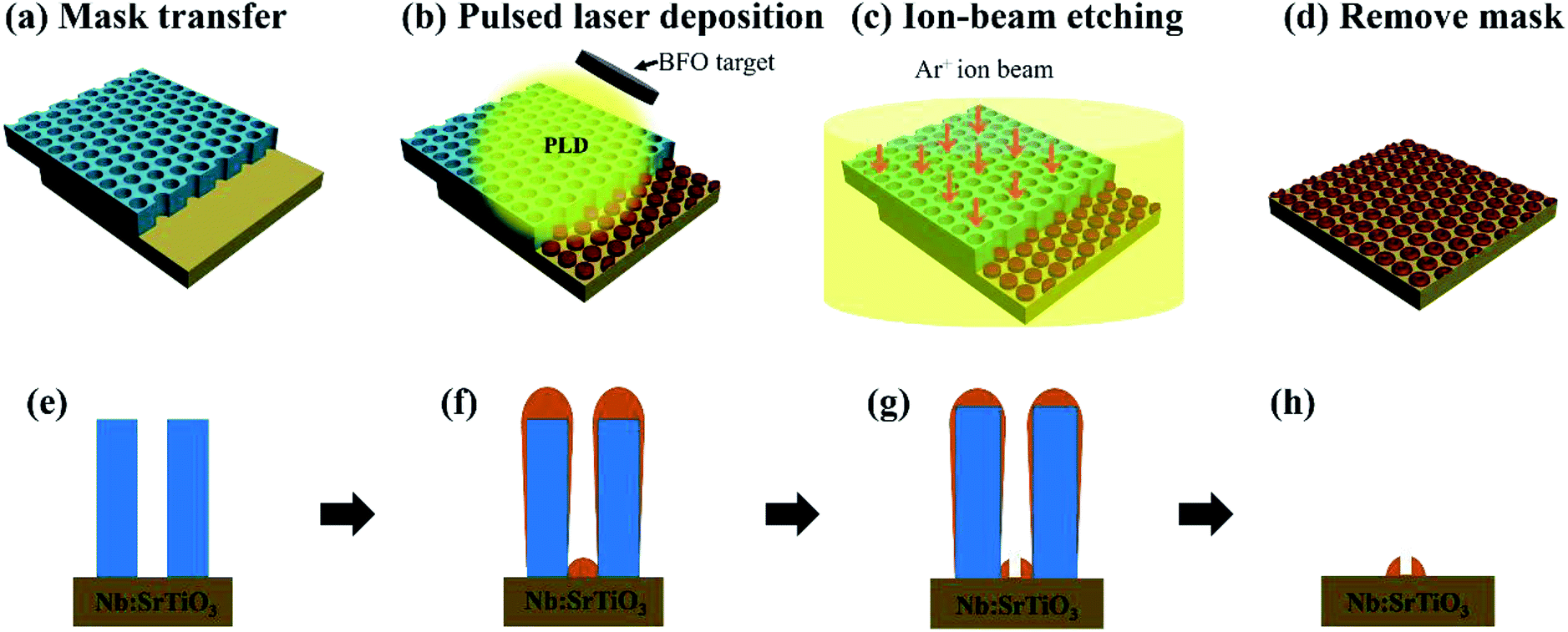
Bifeo 3 Nanorings Synthesized Via Aao Template Assisted Pulsed Laser Deposition And Ion Beam Etching Rsc Advances Rsc Publishing Doi 10 1039 C7ra07677k
Pdf Etching Magnetic Tunnel Junction With Metal Etchers
Https Backend Orbit Dtu Dk Ws Files 99357008 Phd Thesis Kristian Hagsted Rasmussen Screen 03042014 Pdf

Pdf Adhesion Enhancement Of Dlc Hard Coatings By Hipims Metal Ion Etching Pretreatment
Https Encrypted Tbn0 Gstatic Com Images Q Tbn 3aand9gctwp99kqmbp6oyyyhgaqxn8yiga4ymkltunwfydax34ccj7uape Usqp Cau
Source : pinterest.com
